(Hong Kong)


Product Summary
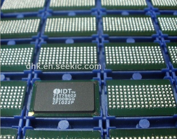
The IDT71T75602S200BGGI is a 2.5V high-speed 18,874,368-bit 18 Megabit) synchronous SRAM. The IDT71T75602S200BGGI is designed to eliminate dead bus cycles when turning the bus around between reads and writes, or writes and reads. Thus the IDT71T75602S200BGGI has been given the name ZBT or Zero Bus Turnaround.
Parametrics
IDT71T75602S200BGGI absolute maximum ratings: (1) Terminal Voltage with Respect to GND VTERM: -0.5 to +3.6V; (2) Terminal Voltage with Respect to GND VTERM: -0.5 to VDD; (3) Terminal Voltage with Respect to GND VTERM: -0.5 V to VDD +0.5V; (4) Operating Ambient Temperature: 0 to +70°C (Commercial), -40 to +85°C (Industrial) ; (5) Temperature Under Bias: -55 to +125°C -55 to +125°C; (6) Storage Temperature: -55 to +125°C -55 to +125°C; (7) Power Dissipation: 2.0W; (8) DC Output Current: 50mA.
Features
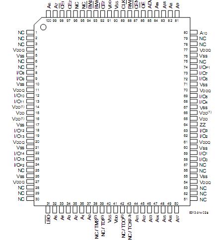
IDT71T75602S200BGGI features: (1) 512K x 36, 1M x 18 memory configurations; (2) Supports high performance system speed - 225 MHz (3.0 ns Clock-to-Data Access) ; (3) No dead cycles between write and read cycles; (4) Internally synchronized output buffer enable eliminates the need to control OE; (4) Single R/W (READ/WRITE) control pin; (5) Positive clock-edge triggered address, data, and control signal registers for fullypipelined applications; (6) 4-word burst capability (interleaved or linear) ; (7) Three chip enables for simple depth expansion; (8) 2.5V power supply (±5%) ; (9) 2.5V I/O Supply (VDDQ) ; (10) Power down controlled by ZZ input; (11) Boundary Scan JTAG Interface (IEEE 1149.1 Compliant) ; (12) Packaged in a JEDEC standard 100-pin plastic thin quad
flatpack (TQFP), 119 ball grid array (BGA) .
Diagrams
| Image | Part No | Mfg | Description |  |
Pricing (USD) |
Quantity | ||||
|---|---|---|---|---|---|---|---|---|---|---|
 |
 IDT71T75602S200BGGI |
|
IC SRAM 18MBIT 200MHZ 119BGA |
Data Sheet |
Negotiable |
|
||||
|
IDT71T75602S200BGGI8 |
|
IC SRAM 18MBIT 200MHZ 119BGA |
Data Sheet |
Negotiable |
|
||||